TSMC Fab Capacity
Overview
This report describes several methods to make rough estimates of the chip production capacity of TSMC on the most advanced nodes, primarily the 5nm and 3nm nodes. These are the nodes used for the most advanced chips, including Apple silicon, Google’s TPUs and NVidia’s most advanced HPC GPUs. Using official statements from TSMC, industry media reports and open source intelligence (OSINT) we describe several methodologies to triangulate these quantities. Ideally we would lke to quantify effective capacity: how much can be actually produced with high utilization, accouting for downtown, yield ramps and maintanence. In practice we identify the installed capacity of the tools and fabs, and scale that by a utilization factor (assumed to be 80%) to account for production factors separate from tooling.
The broader aim of this project is to quantify global chip fabrication capacity. Chips are an essential input for AI, so chip fabrication capacity is one way to understand the limits on AI scaling.
However, the bulk of the chips used in AI are currently manufactured by NVidia, and NVidia uses TSMC as their primary fab for manufacturing the chips. Google and AMD also currently use TSMC as their primary fab. So focusing on the most advanced nodes at TSMC is a reasonable place to start.
This project describes three approaches. First using TSMC’s earnings reports and public information about wafer pricing, we estimate TSMC’s actual production by node. Second, using ASML’s earnings reports, we estimate which global fabs possess the most advanced lithography scanners. Using the specifications listed for ASML’s product lines, we estimate capacity. Finally, using satellite imagery and industry reports, we estimate the energy usage of two of TSMC’s advanced fabs, and use this to estimate production capacity.
The results are reasonable and robust. This report’s production estimates are within 10% of reported wafer production for all quarters within the analysis. This report’s capacity estimates for advanced nodes (7nm, 5nm, 3nm) is within 10% of the capacity reported by TSMC for their four GIGAFAB’s. These fabs are responsible for the production of substantially all of the advanced nodes, though its unclear how much of the capacity in the GIGAFAB’s is for legacy nodes. The time series of production capacity broadly aligns with the capacity reported by other industry analysts.
Commercially Available Supply Chain Analysis
Given the important role that semiconductors play in industry, and the growing importance of AI, there are a number of organizations and analysts who sell research reports estimating all aspects of the semiconductor supply chain. This includes sector analysts at investment banks and buy-side investment firms, as well as industry consultants. Undoubtedly the approaches described in this research report are not novel. However, they depend only on publicly available information and they are replicable.
This project encompassed approximately 70 hours of chatbot-assisted research. However, the author is not a professional supply chain expert. Undoubtedly the research available commercially is deeper, more comprehensive, and be based on sources which are private or which the author was unable to locate. On the other hand, commercial research reports generally may not be republished, whereas the methods here are open and based on public data.
Here is a list of some firms which sell semiconductor supply chain analysis related to fab capacity:
- SEMI is the non-for-profit industry trade group for the semiconductor industry. One of their flagship products is the fab forecast.
- Knometa also publishes research reports on manufacturing capacity, though their final report was in 2024
- Tech Insights publishes reports on many aspects of the semiconductor supply chain
- Counterpoint Research is another semiconductor supply chain research firm
Quantifying Wafer Production
The industry standard production unit is “wafers per month” which refers the number of finished silicon wafers produced in one month. A wafer is a thin silicon disc which is etched and doped to produce many individual semiconductor chips. After wafer production, there are other stages of production which involve cutting the wafer into individual chips and packaging the chips, and assembling them onto circuit boards and devices. Modern nodes are etched onto 300mm (~12”) diameter wafers. Sometimes capacity and production is reported in 300mm-equivalents to convert production of older 200mm (~8”) diameter wafers into a comparable unit.
Increasingly elaborate engineering techniques have been developed to make chips smaller, faster and more capable. The most advanced chips use a methodology called Extreme Ultraviolet (EUV) lithography, where a laser vaporizes a droplet of tin, and the resulting plasma emits light at a wavelength of 13.5nm. The light is reflected through a reticle with a mask, then focused on the silicon wafer surface. The surface has been coated with photoresist which reacts when exposed to light. Subsequent stages remove the photo resist and etch the silicon with the patterns from the mask. For modern nodes, the same wafer is may be exposed and etched several times to make the final pattern.
Different generations of technology are grouped into “nodes”. The nodes originally represented a physical property of the size of the patterns etched into silicon, but this is no longer the case. However, the tradition of naming nodes after a length-scale continues. The most advanced high-production nodes are currently 5nm and 3nm, though research is being conducted into 2nm and 1.7 angstrom (A17) nodes. Different firms use different marketing terms, and nodes are not always directly comparable between firms. Industry reports sometimes distinguish their manufacturing process with additional modifiers, so you will see nodes described as “N7+” or “N3E” where the “E” stands for “enhanced”. In this research note, for lack of more finely grained data, we will set aside some of these these distinctions and use node labels like “7nm”, “5nm” and “3nm”.
Production Capacity Reported by TSMC
TSMC does not directly report production capacity in fine detail, such as at the fab or node level. However, the official sources do provide some high-level statistics which anchor this analysis.
At the end of 2024, across 4 GIGAFAB facilities (fab 12, fab 14, fab 15 and fab 18) which comprise the bulk of advanced node manufacturing, TSMC reports an annual capacity of 12.74 million 300mm-equivalent wafer capacity, which translates to 1,061 kwpm. source
Annual production capacity for all of the manufacturing facilities managed by TSMC and its subsidiaries was approximately 17 million 300mm equivalent wafers and the end of 2024 (~1,400 kwpm). source
The 2024 annual report states that total wafer shipments were 12.9 million 300mm-equivalent wafers as compared to 12.0 million 300mm-equivalent wafers in 2023. This implies a utilization rate of ~75%.
Furthermore it states the total annual capacity is:
| Year | Capacity |
|---|---|
| 2023 | 16-17 million |
| 2024 | 16-17 million |
| 2025 | 17-18 million |
TSMC Wafer Production
As a lower bound for production capacity, we seek to estimate the actual production. Understanding actual shipments is also useful for quantifying the capacity of AI firms farther down the supply chain. Our approach is rooted in the quarterly earnings statements published by TSMC for investors.
Short outline of the methodology:
- Use earnings report attribution to get sales numbers by node
- Estimate wafer prices using industry reports to convert sales numbers to unit sales
- Compare total sales across nodes to sales reported in earnings
- Adjust the prices using broad semiconductor price indices
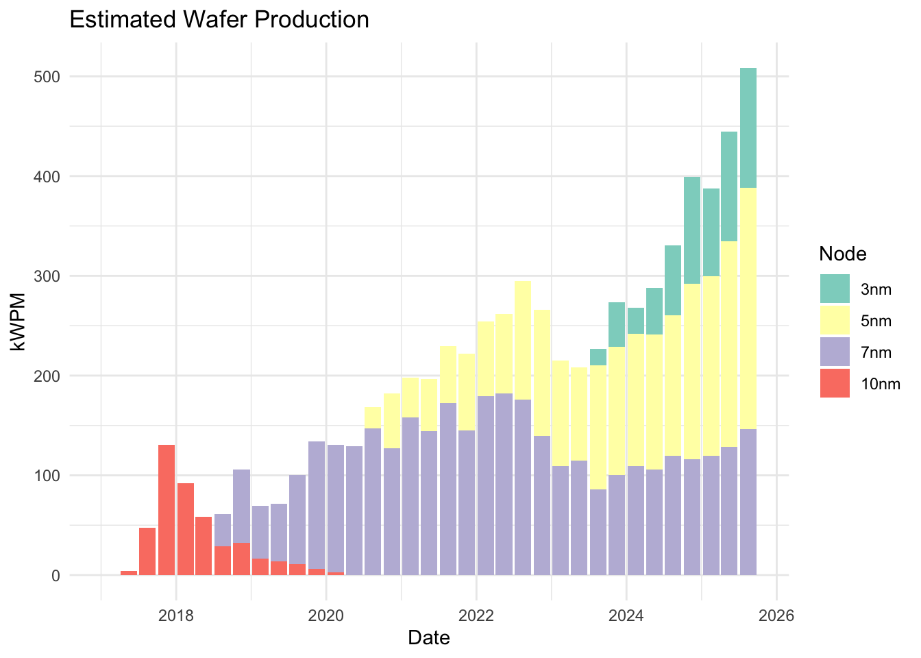
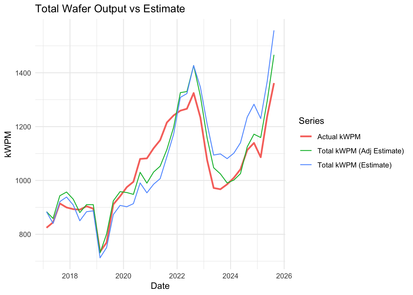
Here are estimates of TSMC wafer production by node over the past 10 years. In subsequent sections we will discuss the various methodologies and assumptions which comprise this approach.
TSMC quarterly reports and revenue attribution
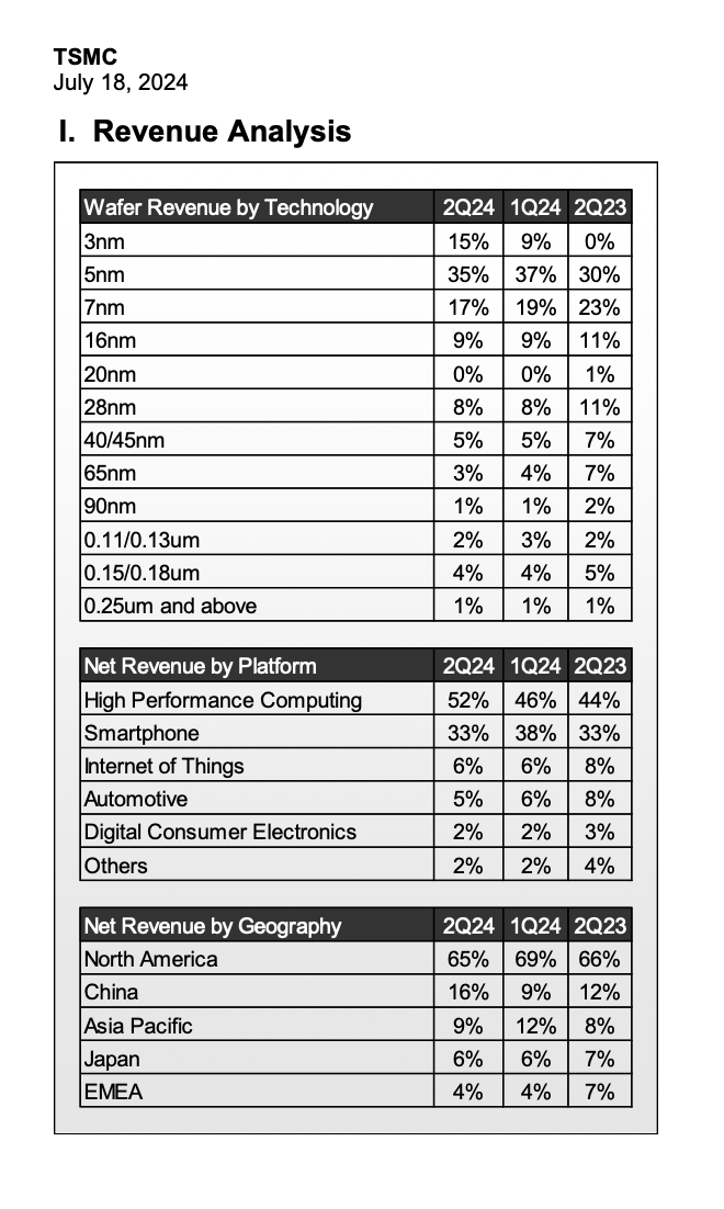
TSMC publishes total wafer production and wafer revenues figures broken out by node type in its quarterly earnings reports. TSMC also publishes the total number of wafers shipments, so this aggregate can be used as a check for our assumptions. This information is available quarterly going back 9 years or so.
In order to translate from sales revenues to number of wafers, we need the average sales price (ASP) for wafers in each category. The remainder of this section will focus on how to estimate the ASP.
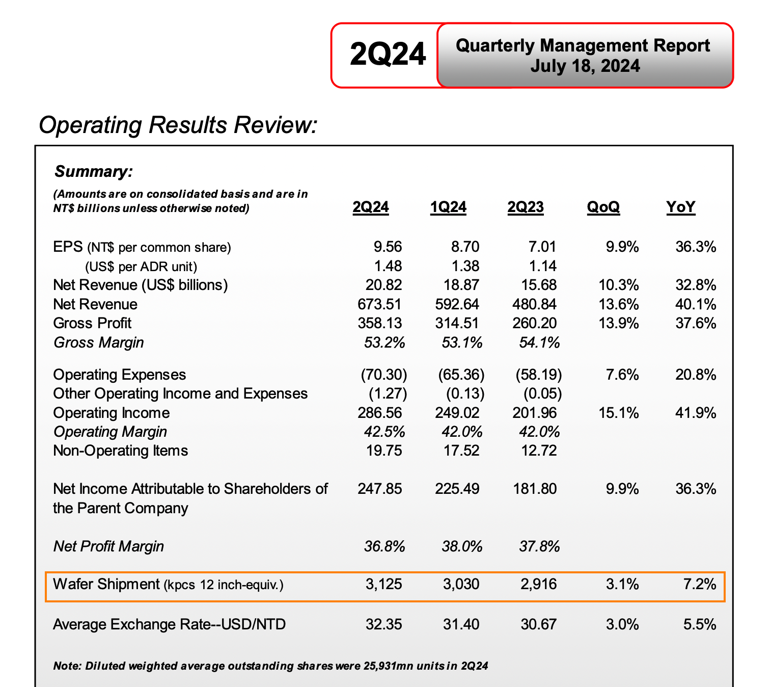
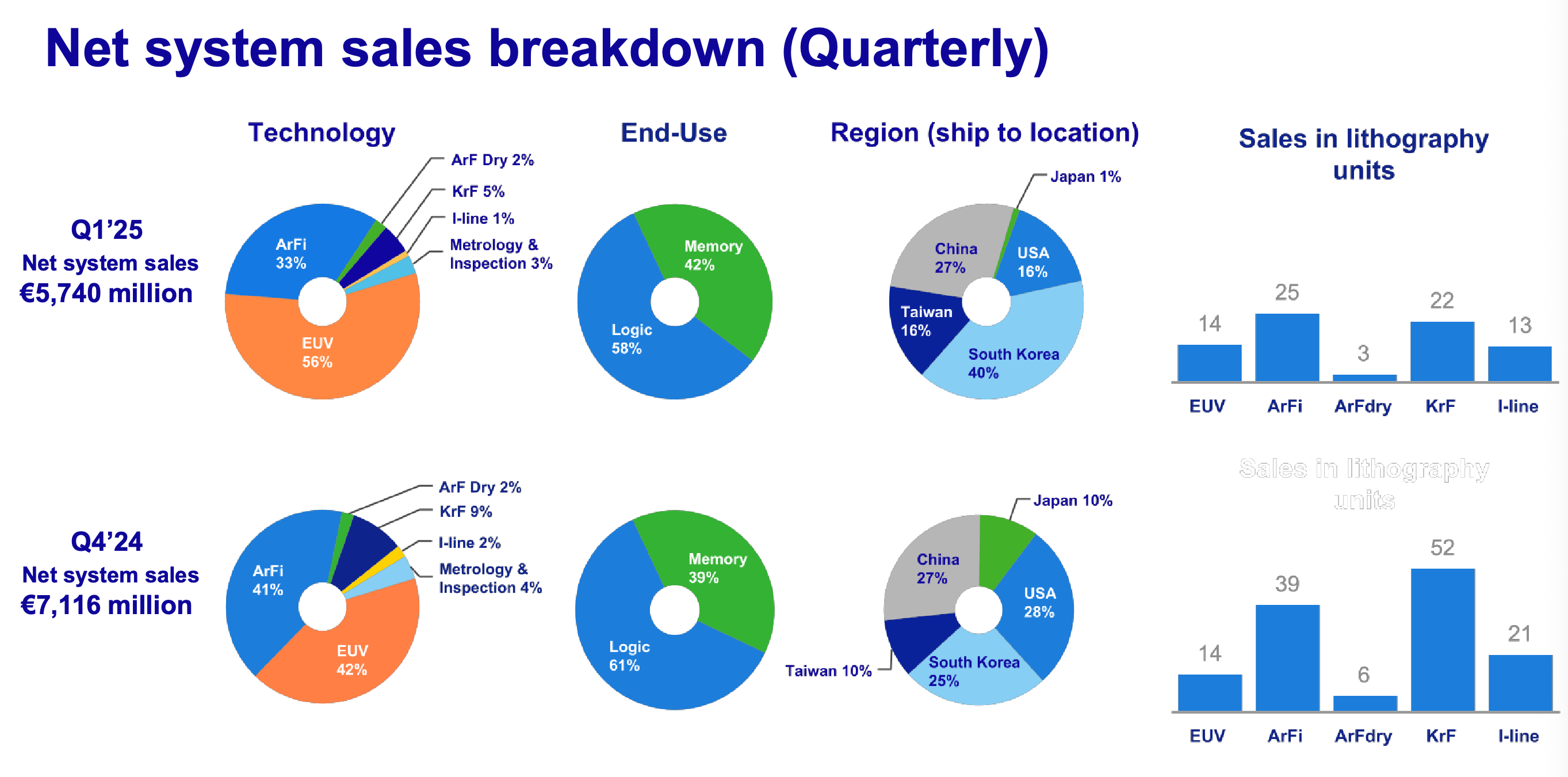
An example of the quarterly reporting published by TSMC is included below.
Average Sales Price (ASP) of Wafers
There are several industry reports which quote estimates of average wafer prices. ASP is an abstraction and isn’t the actual price offered by TSMC. Finished wafer prices are individually negotiated by each customer. These contracts may depend on many details such as the size of the batch, the complexity of the chip, and supply-and-demand for the tooling required to manufacture the specific chip’s specs.
As a Taiwan-based company, TSMC reports its earnings in Taiwan dollars (NT$). However, as silicon wafers are a global commodity, it’s reasonable to assume that prices are more commonly negotiated in US dollars, and that the prices in dollars are more stable. This analysis uses dollar revenues.
- In late 2022, a report by DigiTimes provided estimates for ASP by node type
- A more recent report by Creative Strategies is more-or-less in line with that, and corroborates the steep increase in price by node.
- AnySilicon published wafer price explanatory article with a curve for wafer price estimates by node.
Synthesizing these sources, we use the following table as a rough anchor for translation of revenue to wafer volume. These are not actual prices, they are assumptions which are inputs to our analysis.
| Node | ASP ($k) |
|---|---|
| 3nm | 20 |
| 5nm | 16 |
| 7nm | 10 |
| 10nm | 6 |
| 16nm-20nm | 4 |
| 28nm | 3 |
| 40nm-90nm | 2.6 |
| 0.1µm+ | 2 |
With these prices, we translate revenues in each node category to wafer shipment numbers. Summing over the quantities in each category yields a total number of wafers shipments which can be compared to the actual reported total wafer shipments. Our ASP estimates are primarily from a source published in 2022, and the total implied wafer production calibrates well (within 5%) to four quarters of 2022.
A comparison between the estimated total wafers shipments and the actual reported total wafers shipments is shown below. Using these prices underestimates production in periods earlier than 2022, suggesting ASPs were lower then, and overestimates recent production, suggesting ASPs are higher. This plot also shows the effects of an adjustment described in the next section.
Adjusting for broad price trends
TSMC adjusts prices up and down according to demand and costs. It raised prices by 10% in 2022, and is poised to raise prices again in 2026. For advanced nodes, TSMC is the primary global supplier and it therefore has significant pricing power. It has stated that its target is sustained gross margins above 50%.
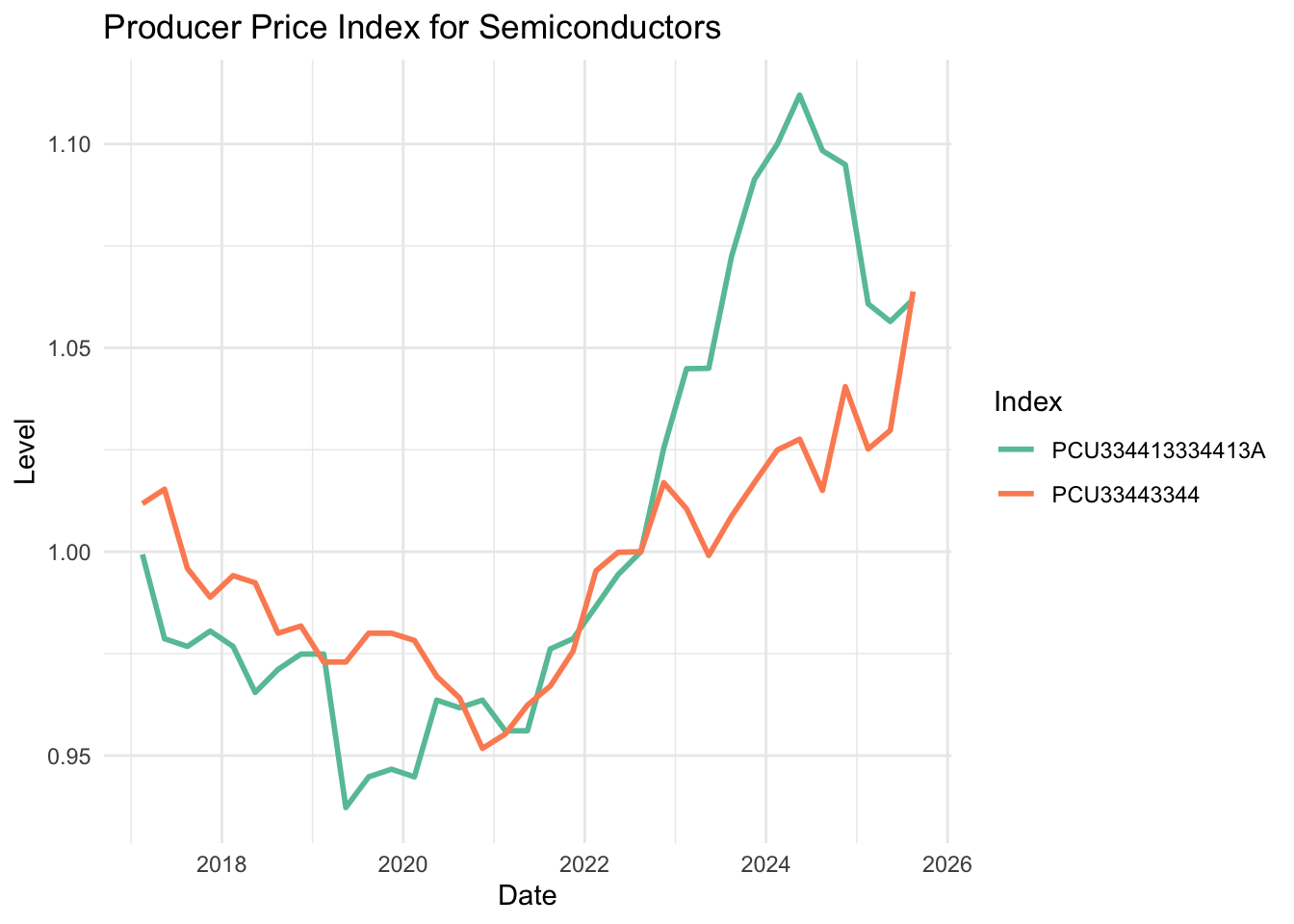
As a proxy for broad price trends, we incorporate the Bureau of Labor Statistics’ Producer Price Index by Industry. Two relevant series are PCU33443344 for “semiconductor and other electronic component manufacturing” and PCU334413334413A for “other semiconductor devices, including transistors, diodes, and semiconductor parts such as wafers”. Both are plotted below, normalized to Q3 2022, the date of the article which anchors our ASPs estimates They show broadly similar trends, though the movements are larger for the more specific series ending in “13A”. We use this more specific series in our analysis. Neither of these series directly reflects the market for finished wafers, but they provide a useful approximation for general price trends.
For each time period, adjust baseline prices over time by changes in the PPI, normalized so that 3Q22 matches the anchor prices in the previous section. This adjustment makes the total output estimated from revenues and ASPs better match the actual total output.
Below is a plot of the change in percent error from making this adjustment.

Regression analysis
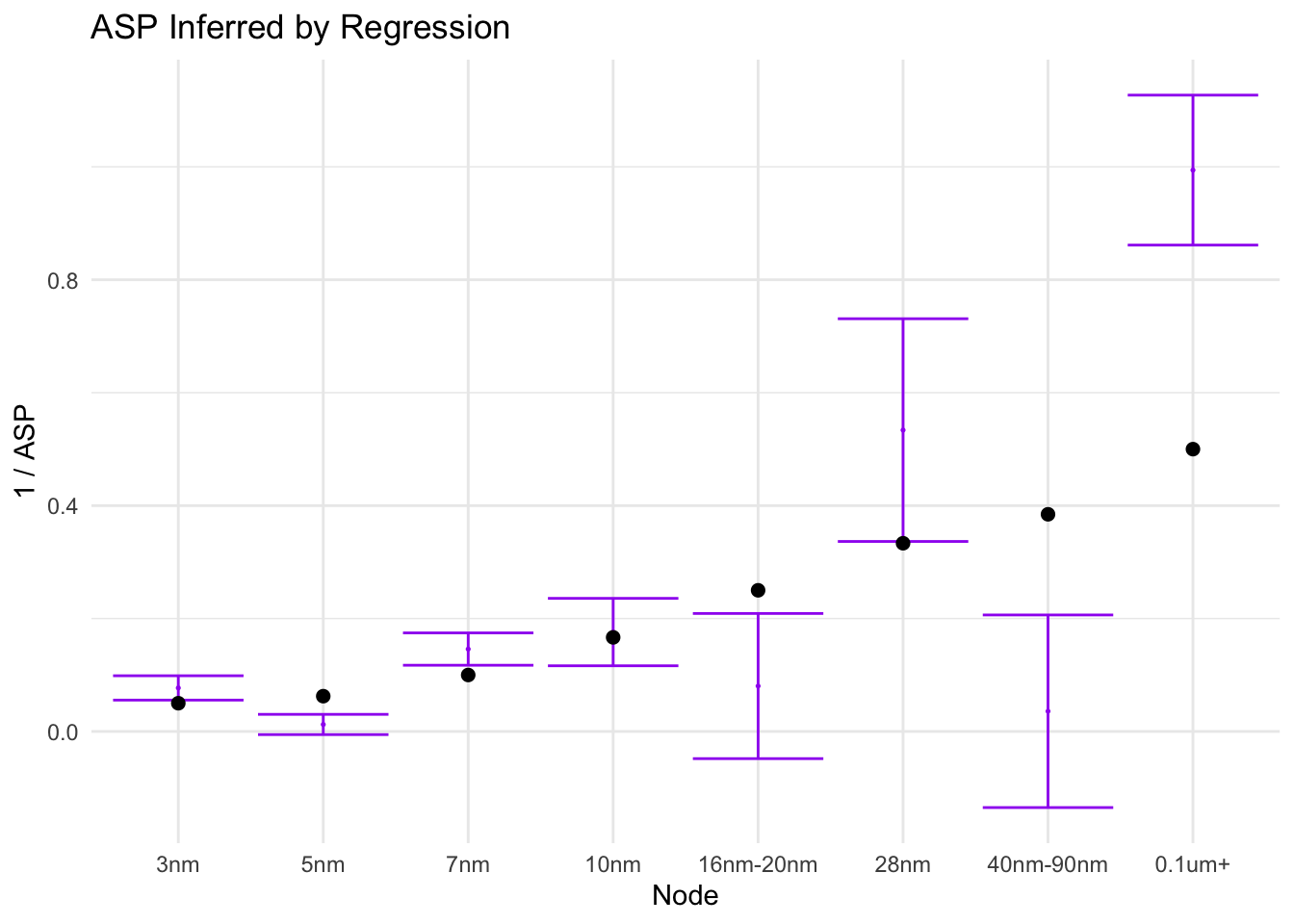
As an additional sanity check for the ASPs, we perform a linear regression of total wafer production against revenues-by-node adjusted by PPI. The regression coefficients should correspond to reciprocal ASPs. Since wafer revenues for the various nodes are all strongly correlated with broad market trends and hence to each other, the regression struggles to identify which nodes should be associated with which revenue changes. Thus, the coefficients are unstable and have large error bars, and the analysis is a bit inconclusive. However, for the advanced nodes it shows the ASPs used for this analysis aren’t wildly off base.
The black points are the ASPs used in this analysis, and the purple lines are the error bars estimated from regression. Note however that some of the error bars for the reciprocal ASPs pass through zero, which implies the error range for the ASPs includes infinity.
Capacity Model: Scanner Delivery Tracking
In this section we discuss the first of two approaches for estimating the manufacturing capacity of TSMC. In the first of two approaches, we track a critical input to semiconductor manufacturing, lithography scanners.
There are a number of critical inputs to wafer production such as: unprocessed silicon wafers, electricity, water, specialized gasses, chemicals used for etching and doping. However, one of the rate-limiting tools for manufacturing is the scanner. This is the machine which uses lasers to imprint the design of the semiconductor on the photoresist. Other manufacturing steps, such as etch and deposition, can also be rate limiting in the manufacturing process for a given chip. For tractability, we will focus solely on scanner capacity.
Modern nodes use extreme ultraviolet (EUV) scanners. ASML is a Dutch company which manufactures lithography scanners. Importantly, is the only global supplier for the EUV lithography scanners used in advanced nodes.
Thus, scanner tracking is a convenient method for constraining capacity because scanners are discrete units relatively small in number. They are expensive equipment costing hundreds of millions of dollars. One may expect that, unlike wafers or gas, it’s not economical to have a large number of stockpiled unused scanners. Because ASML is the only global supplier of EUV scanners, it is possible to estimate scanner sales by analyzing just one company.
This model will implicitly assume that once a scanner is delivered, it is productive in a short predictable window. In reality there is a longer process of testing and ramp up before scanners are producing at maximum capacity. Also this model abstracts away a lot of details about specific scanner installations in specific plants for specific workloads. In that respect, it assumes that scanner hours are essentially fungible. In reality particular scanners are installed in specific locations as a part of a larger production tool chain and may be purposed in specialized ways which would limit overall capacity. The model does not explicitly track fab-level constraints, customer-specific allocations, or short-term imbalances.
Results
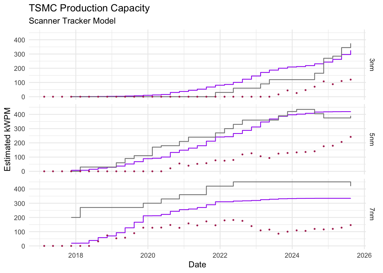
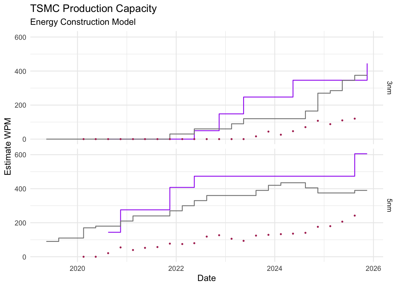
Here are the results of the model. The throughput refers to finished wafers per hour, accounting for multiple exposures (discussed later).
Short outline of the methodology:
- Use reported ASML earnings breakdown to estimate scanner sales revenues from TSMC
- Use average sales price data to convert revenues to units by scanner product model
- From reported specs of scanner models and assumptions about exposure numbers and efficiency, estimate wafer capacity.
The maroon dots represent actual estimated production numbers from the previous section. The purple line is the result of our model. The grey line is the estimate of another industry analyst for reference and comparison.
ASML quarterly reports and revenue attribution
While ASML does not report exactly which scanners it has sold to which customers, it does provide some granular breakdown of its sales figures in its quarterly financial statements.
In particular, ASML reports the percent of revenues by the technology type (EUV, ArFi, etc.) of the scanner, and the percent of revenues by region (Taiwan, China, etc.). An example of their quarterly report revenue breakdown is included below. This simplifies our problem because the major consumer of lithography machines in Taiwan is TSMC. While TSMC is building capacity in other countries, these projects are relatively small and nascent compared with the GIGAFAB’s currently in operation in Taiwan. Thus, the bulk of its advanced node production and hence the location of its EUV scanners is in Taiwan. So as an approximation, we take the ASML sales revenues attributed to Taiwan as consisting of the total sales to TSMC.
Conceivably this analysis could also be extended to Samsung, which is the major producer of chips in Korea and whose fabs are all located in Korea. Intel’s global fab footprint is more complicated, but with additional assumptions this analysis could potentially be extended to that company as well.
Note that ASML reports on scanner deliveries, whereas we would prefer to know when scanners are fully operational. Furthermore, this approach cannot track scanner retirement, or scanner install-base from before when the analysis begain.
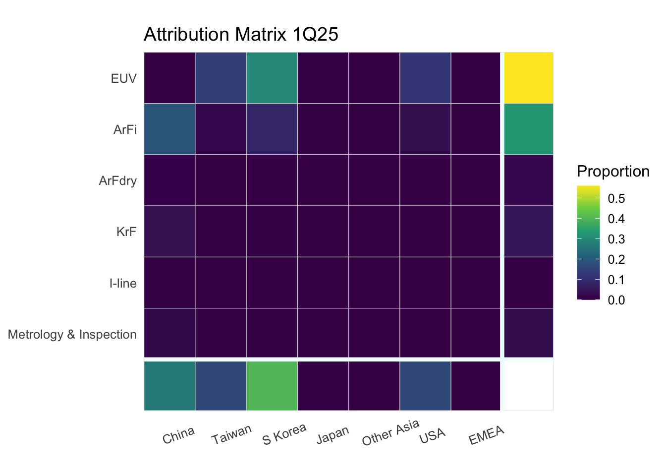
Since ASML publishes a breakdown of both units and revenues by technology type, we can infer the ASP of each technology type. What we would like is the joint allocation of units between technology type and region. However, we only only given the marginal allocation: revenues share by region and revenue share by technology type, so additional assumptions are needed.
“Raking” the Revenue Allocation
Iterative Proportional Fitting (IPF) is a technique for finding a joint distribution \(M\) which is closest to an initial non-negative matrix \(P\) which also matches specified marginal distributions. Closeness here is measured by KL-divergence. Because IPF alternately adjusts the output to match the marginal distributions in one dimension and then the other, this technique is sometimes called “raking”. We will use this technique to get a reasonable cross-table of scanner revenue by region and technology type.
By adjusting the relative strength of the entries in \(P\), we can crudely encode some of the known “priors” about the allocation of scanners. If the initial matrix \(P\) is the matrix of all 1’s, then the results of IPF \(M\) are just the independent distribution. That is, the entries in the table are the product of the entries on the margins. If the initial matrix has 0’s in some entries, then the result will also have zeros in those entries. An alternative approach which would allow more precise quantification of uncertainty would be to run a full Bayesian program with more explicit and detailed priors. However, IPF is straight forward, easy to implement and gives reasonable results.
We know that owing to export controls, EUV machines and some advanced argon flouride immersion (ArFi) scanners are not sold to China. We also know that among all chip manufacturers, TSMC has been an early adopter and large purchaser of EUV scanners.
Taking these considerations into account, we set the initial matrix to have an relative strength of 0 for EUV scanners in China, ½ for ArFi scanners in China, 2 for EUV in Taiwan, and 1 for all other entries.
Here is an example of the resulting attribution matrix for the 1Q25 earnings report included above. The boxes at the bottom and the side represent the marginal fraction of revenues for that category, which come directly from the ASML earnings statement. The 6x7 grid in the center represents the inferred revenue allocation from IPF using the assumptions embedded in our initial matrix.
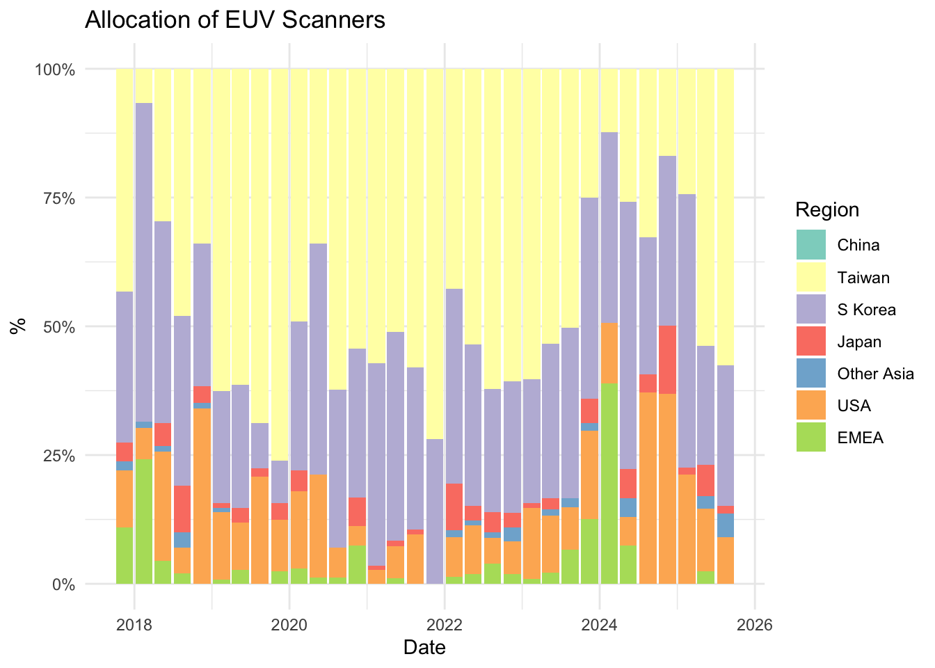
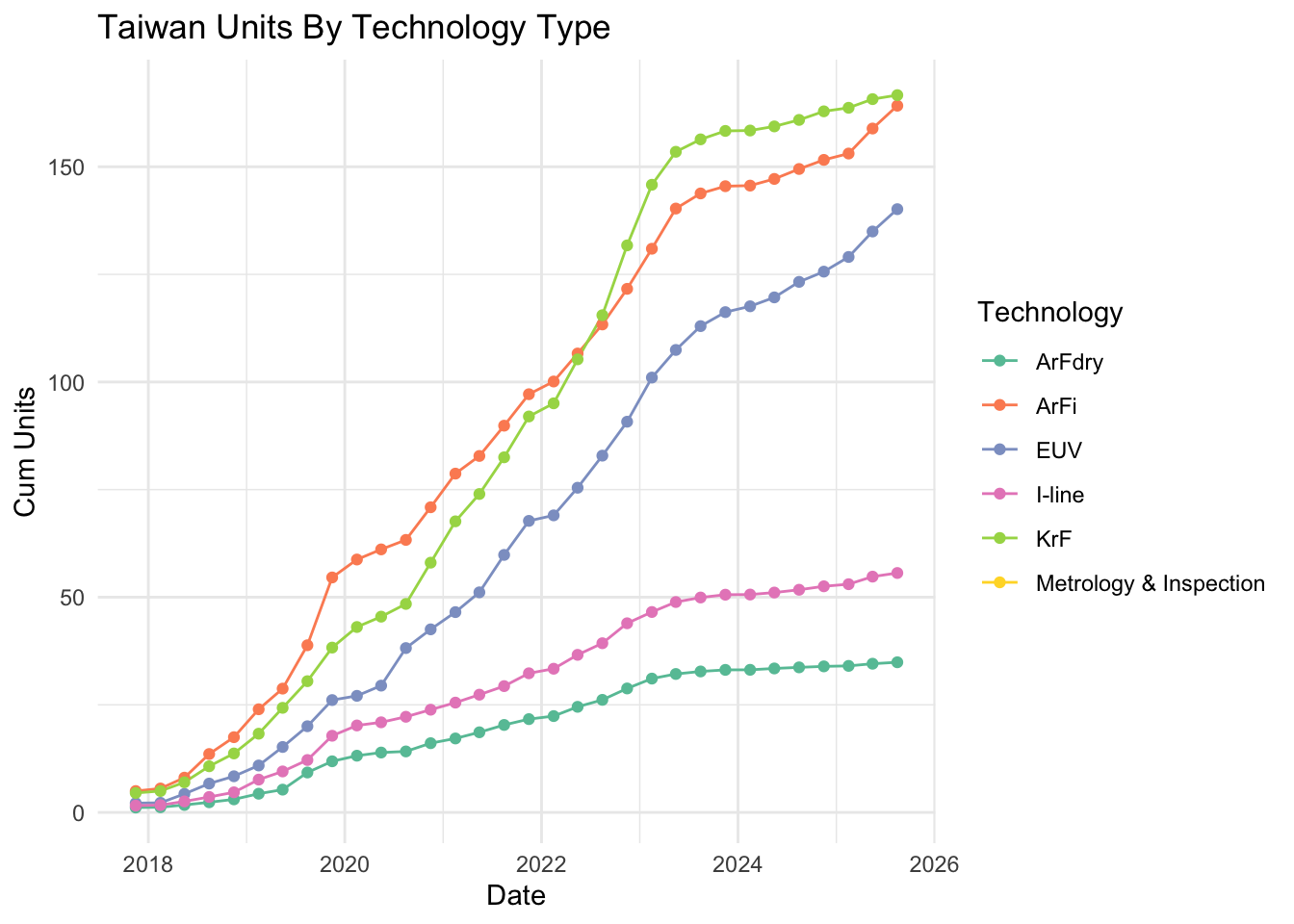
Here is the revenue allocation of EUV scanners by region over time.
ASP and Unit Allocation
Rather than revenue allocation, we would like to know the allocation of scanner units. At this stage of the analysis, we are only focusing on total EUV scanner counts, and ignoring specific product models. However, the operational details of different EUV product lines will be relevant for throughput analysis. We will refine the analysis in the next section.
As a simplifying assmption, presume that all regions purchase scanners within the same technology category at the same ASP. This is unrealistic, as its likely that early adopters of advanced nodes like TSMC will buy more expensive leading edge models within a category and will have a higher ASP. However, absent data to quantify differences between regions, we ignore this distinction.
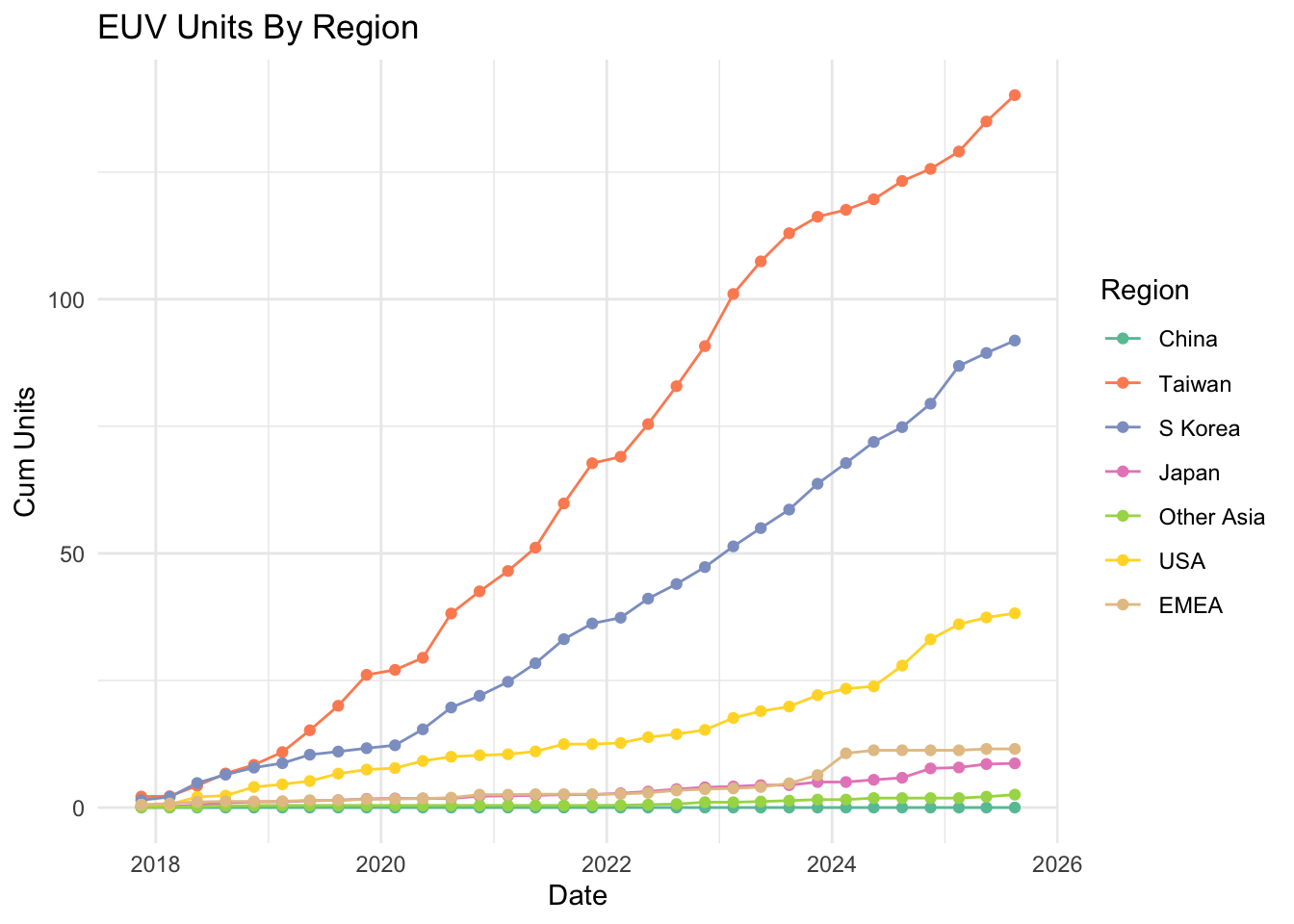
As stated previously, we assume all scanners delivered to Taiwan are TSMC scanners, and all scanners delivered elsewhere are not TSMC scanners. This is not strictly true. Notably TSMC is building an advanced node GIGAFAB in Arizona which is starting to come online. Furthermore, TSMC has joint ventures for legacy nodes in Japan, China, Washington State, and a planned joint venture in Europe. Within the limits of uncertainty of the other assumptions of this model, this is a reasonable starting place.
At a 2024 Technology Symposium, TSMC announced that they had 10x more EUV scanners in 2023 than in 2019 and that they had 56% of the global installed base of EUV scanners. This is consistent with the our results. According to the model, TSMC had 11 scanners in Q1 2019, and 113 in Q3 2023, a 10.2x increase. Furthermore, according to the model in Q3 2023 TSMC’s EUV scanners are 56% of the total (113 out of 202).
EUV Scanner Throughput
All of the most advanced nodes use EUV scanners. However, within the EUV technology segment there are a number of different product lines, and different models are used to manufacture different nodes. We will assume that TSMC uses the models NXE:3400C, NXE:3600D and NXE:3800D for its EUV node production. In the recent past, ASML manufactured other EUV models such as the NXE:3350B which are currently discontinued. For simplicity we’ll focus on the current models whose specs are easier to obtain, and whose functions are more clearly differentiated. ASML also manufactures next generation High NA EUV machines, such as the EXE:5000 and the EXE:5200B. However, at industry symposia, TSMC has stated it does not yet use this technology for mass production, only for R&D.
From industry reports and product specification pages, we make the following assumptions about which scanners are used for which nodes by TSMC. The relationship between nodes and product lines doesn’t exactly match the descriptions on the product specification pages. In general, ASML marketing material tends to associate nodes with more advanced models than reporting from TSMC suggests they actually use. Here are some industry reports on the manufacturing process for 7nm, 5nm, and 3nm nodes which give indications of the scanner models utilized.
| Technology | 2nm | 3nm | 5nm | 7nm | wph | specs |
|---|---|---|---|---|---|---|
| NXE:3400C | 50% | 50% | 135 | specs | ||
| NXE:3600D | 50% | 50% | 160 | specs | ||
| NXE:3800E | 100% | 220 | specs report | |||
| EXE:5000 | 100% | 185 | specs | |||
| EXE:5200B | 50% | 175 | specs |
The specs for each model include the throughput measured in “wafers per hour” (wph) at 100% utilization. ASML’s wafer per hour numbers refer to a single exposure step, whereas finished wafers have multiple exposure and etch cycles. In fact, the manufacturing of advanced nodes has seen the marked increase in the number of exposures required to manufacture a chip. Mutiple exposures allow for details to be etched on mutiple physical layers, and also exposures of related masks can allow for layouts to achieve a finer pitch. In terms of throughput, we need an estimate for the typical number of exposures for a finished product, and industry shorthand which encompasses a number of different manufacturing processes is the number of “layers”. Sometimes a technical distinction is made between “layers” and “exposures”. For the purposes of this analysis, the number is just a factor for converting the wafer per hour throughput listed in the scanner spec to a rate of finished wafer throughput. Throughput is simply the ASML spec throughput divided by the average number of EUV exposures required per wafer, for which we use the industry shorthand “layers”.
The number of layers depends on the particular semiconductor being produced and is not universal to a node. Logic semiconductors tend to require more layers than memory semiconductors, and HPC / AI products have more layers than mobile phone SoC products. Some sources distinguish manufacturing processes into finer categories, such as “N3” as compared with “N3E”. This analysis abstracts away these details, focusing on the average number, but these distinctions could be important for forcasting chip capacity for AI usage. In any case, the trend toward increasing numbers of scans for advanced nodes is an important factor in manufacturing capacity, and we make some simplifying assumptions listed below.
Here are the approximate number of layers by node, which are used as a modeling input.
| Node | Layers | Source |
|---|---|---|
| 7nm | 4 | Tom’s |
| 5nm | 12 | wikichip |
| 3nm | 22 | semianalysis |
| 2nm | 25 | Tom’s |
The final factor important for estimating scanner output is the overall efficiency. Scanners are not always operating at peak capacity. This can be for a variety of reasons, including planned and unplanned maintanence, rescans due to defects or overlay failures, the time taken to swap reticles, or delays in other stages of manufacturing. From industry news and annual reports, we estimate this factor to be around 80%.
ASP and Product Line Allocation
As ASML only reports revenues by broad technology type, we need additional assumptions to determine which scanner models are operated by TSMC. One clue is to look at trends in scanner ASPs over time. The ASP for the EUV line has increased almost 2.5x over the time period of this analysis. On an earning call with investment analysts, ASML management have discussed how the product mix is affecting the ASP.
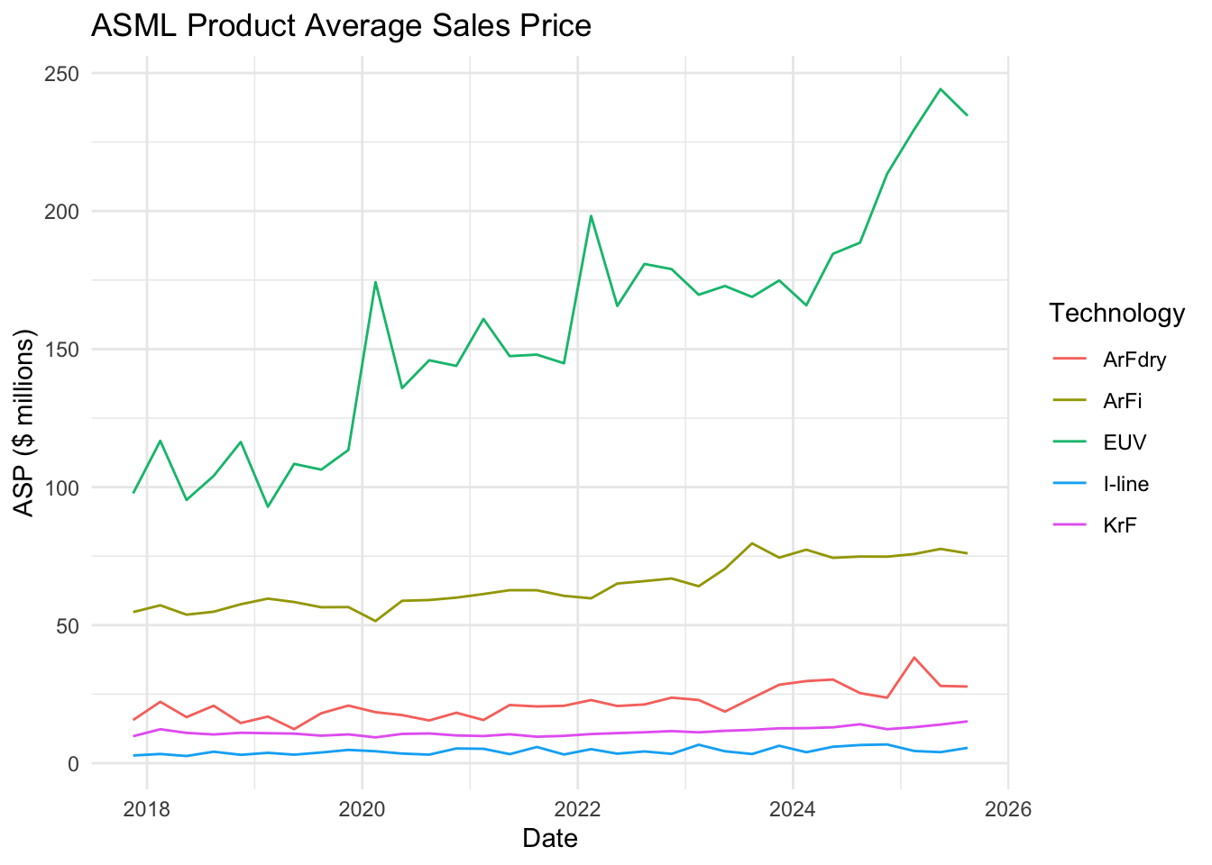
Below is an estimate of the ASP of particular scanner models. There are a lot of sources of uncertainty in these estimates. First, public reports about scanner prices are sketchy and approximate and rarely mention specific models. Almost certainly, product lines and their prices have changed over time. As mentioned previously, ASPs for TSMC are likely higher than the overall reported ASP as they are early adopters of advanced scanner technology.
| Model | Price | source |
|---|---|---|
| NXE:3400C | $120mm | wikichip |
| NXE:3600D | $160mm | reuters, ft |
| NXE:3800E | $230mm | earnings call |
| EXE:5000 | $350mm | reuters |
| EXE:5200B | $350mm | reuters |
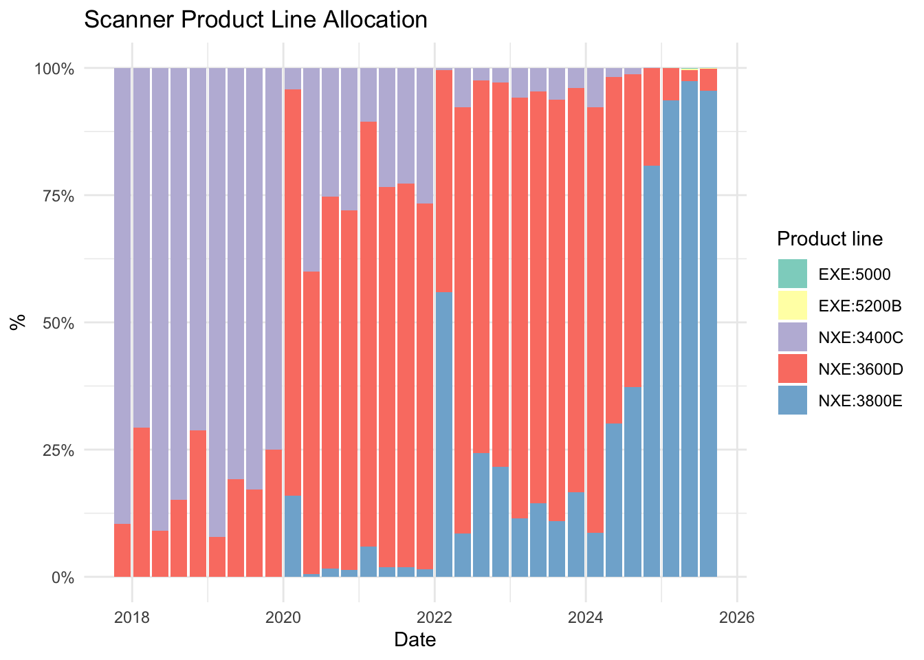
Using Nadaraya-Watson kernel regression we decompose the EUV segment ASP to provide weights to each product line using the above price points. Linearly interpolating between neighboring price points gives very similar results, but kernel regression is a bit smoother. Using these weights, we allocate the units within the EUV segment to specific scanner models. The results are shown below. The transitions between scanner product lines roughly correspond to published reports about the adoption of 5nm and 3nm technologies.
Capacity Model: Energy and Construction Analysis
In this section we describe a different approach to estimating TSMC production capacity. In order to manufacture of advanced nodes, TSMC has constructed many new fabrication plants. The construction proceeds in phases, and an examination of satellite imagery suggests the design of the each phase is substantially similar. From the observable elements of the construction, namely the cooling towers, we estimate the electrical power usage of the fab and hence the number of scanners it can support. The progress of construction gives a time series of production capacity.
Short outline of the methodology:
- Use satellite imagery and industry reports to track construction at fabrication plants
- Use satellite imagery and industry reports to estimate power consumption
- From estimates of the energy usage of specific scanner models, estimate production capacity
Results
Here are the results of the model. In subsequent sections we will discuss the methodologies and assumptions used in this approach.
TSMC Global Fabs
From company announcements and press reports, it is possible to identify which nodes are produced at which physical fabrication plants. For 3nm and 5nm production capacity, we need to only to focus on Fab 18 in Tainan TW and Fab 21 in Phoenix AZ. The Arizona fab is just now coming online, so the majority of production capacity is currently located in Tainan.
| Location | Fab Name | Nodes | Scanner Model | Source |
|---|---|---|---|---|
| Tainan (STSP) | Fab 18 (GIGAFAB) | 3nm, 5nm | NXE:3600D | TSMC1, TSMC2 |
| Taichung (CTSP) | Fab 15 (GIGAFAB) | 7nm, 28nm | NXE:3400C/3600D, NXT:2000i/2050i | TSMC1, TSMC2, wccftech |
| Phoenix, AZ | Fab 21 | 5nm | NXE:3600D | Tom’s Hardware |
| Hsinchu (Baoshan) | Fab 20 | 2nm | NXE:3800E (?) | TSMC |
| Kaohsiung | Fab 20 | 2nm | NXE:3800E (?) | TSMC |
Fab Phase Construction Timing
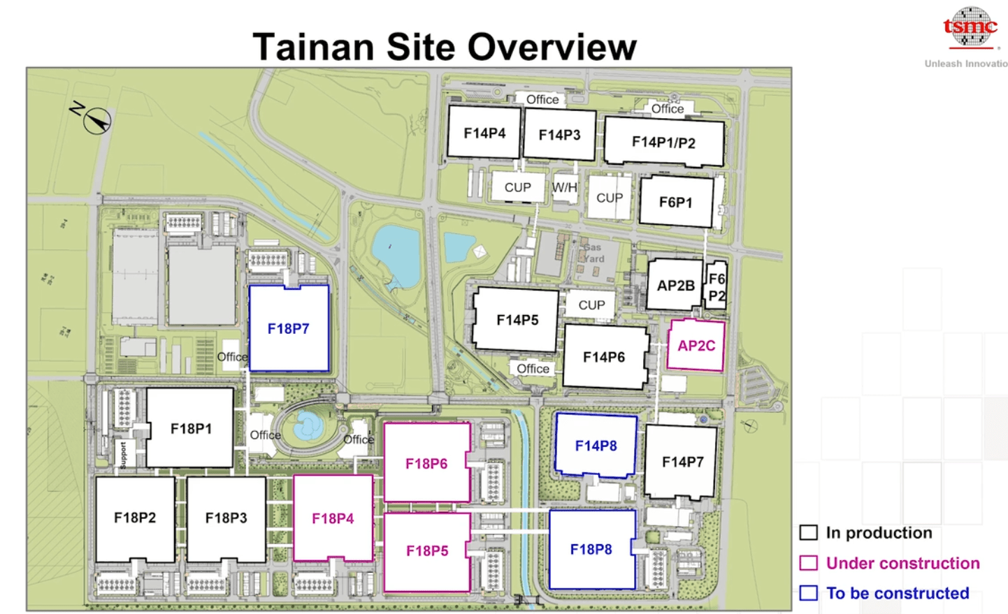
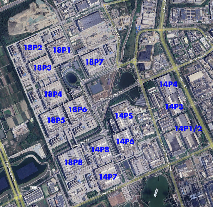
Fab 18 consists of 8 nearly identical buildings, each of which comprises a “phase” of construction and operation. Its located at Hsinchu Science Park in Tainan, Taiwan, which also houses Fab 14. Below is a site map of Tainan from 2021 and a recent satellite photo annotated with labels of the construction phases. The site map labels phases as operational, under constructed, or planned future construction, so this helps us bound the dates of when various phases come online.
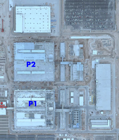
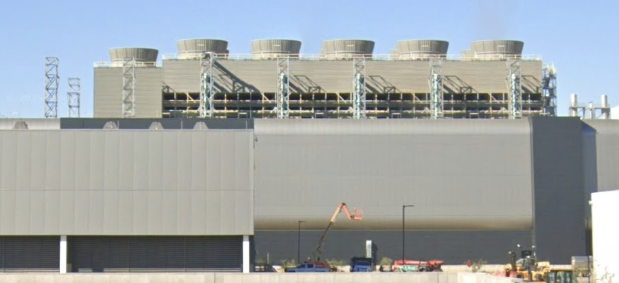
Here is a satellite photo of the TSMC Fab 21 Arizona site, where phase 1 is complete and phase 2 is under construction. The shape and dimensions of the buildings at Fab 21 are essentially the same as the Tainan building phases. Notably, the cooling towers appear to be identical.
Using time-lapse photographs from Google Earth and reports in the press, we are able to assemble a rough timeline for building construction. Unfortuantely Google Earth contains large time gaps in its history of Tainan, so higher quality source of satellite images could greatly improve these estimates. From satellite imagery, it’s not possible to tell at what stage production ramp-up a particular fab is in after the exterior structure is completed, but the imagery does provide a lower bound on when a particular fab is operational. We supplement the imagery with press reports and official corporate announcements about production at various phases.
| Fab Name | Location | Node | Map appearance | Map completion | Reports | Source | |
|---|---|---|---|---|---|---|---|
| Fab 18 P1 | Tainan | 5nm | 2/18 | 12/19 | 1H20 | media 1 | |
| Fab 18 P2 | Tainan | 5nm | 5/18 | 4/21 | 2H20 | media 1 | |
| Fab 18 P3 | Tainan | 5nm | 5/18 | 4/21 | 2H21 | media 1 | |
| Fab 18 P4 | Tainan | 5nm/3nm | 4/21 | 10/21 | 1H22 | SEMI, TSMC p212 | |
| Fab 18 P5 | Tainan | 3nm | 4/21 | 1/22 | 2H22 | SEMI | |
| Fab 18 P6 | Tainan | 3nm | 4/21 | 3/24 | 1H23 | media 2 | |
| Fab 18 P7 | Tainan | 3nm | 10/21 | 3/24 | 1H24 | TSMC | |
| Fab 18 P8 | Tainan | 3nm | 1/22 | 3/24 | 2H25 | media 3 | |
| Fab 21 P1 | Phoenix | 5nm | 5/21 | 2/24 | 2H25 | TSMC | |
| Fab 21 P2 | Phoenix | 3nm | 4/22 | 1H28 | TSMC |
Fab Phase Power Analysis
The energy requirements of a modern fab are substantial. By some estimates, TSMC consumes 9% of all power in Taiwan.
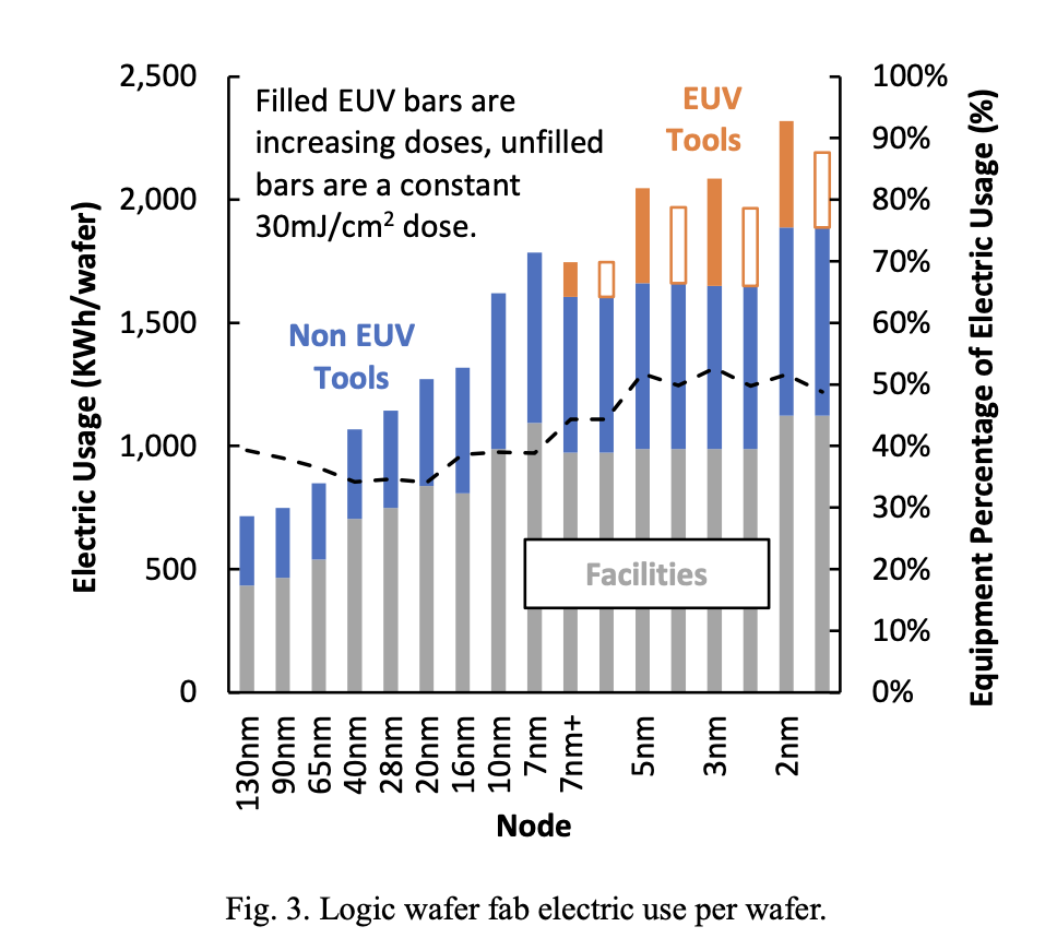
To within an order of magnitude, the electricity consumed by a fab becomes heat which must be ejected to the external environment. Thus by analyzing the capacity of the cooling system, we obtain an estimate for the electrical power consumed. According to Jones 2023 approximately half the energy of a modern fab is used for facilities. This includes HVAC for filtering and conditioning air for clean rooms, fan motors on cooling towers, compressors, pumps, lighting, and other systems.
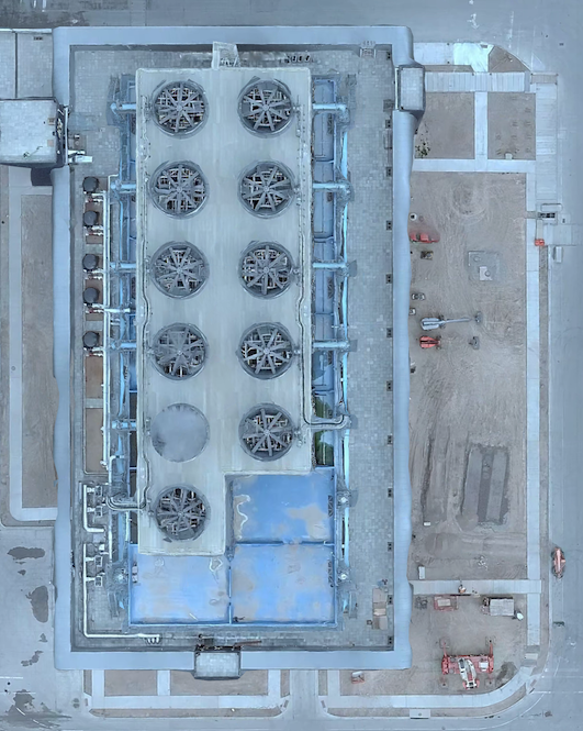
Outside of each phase of fab 18 and fab 21 is a large cooling tower. Below are images of the towers at Fab 21, but the structures at Fab 18 have identical dimensions. Most of the phases in both sites have 11 towers, though the first structure, Fab 18 Phase 1, has 12. Depending on fan velocity and weather conditions, each cell could eject between 12-20 MW of heat energy. Taking mid-range numbers, a tower with 11 cells such as the one pictured could eject ~180MW of energy. The cooling system itself (fans, pumps and condensers) could consume another 10-20MW.
Public reports of the electrical usage of the Arizona fab phase 1 suggest the fab will consume 200MW of power, scaling to 600MW when further phases are constructed. This jibes with the estimtes above.
This could undoubtedly be refined, but as a starting point we will assume each phase consumes 200MW of electricity.
Scanner Power Analysis
TSMC does not report exactly which scanners are used in each fab, though a flythrough video released by TSMC of the interior of Fab 21 shows what industry analysts identify as NXE:3600D’s. This is one of the machines previously associated with 5nm and 3nm production, so this is consistent with the reported production of 5nm semiconductors at Fab 21.
EUV tools are the most energy intensive tool in the fab, but even so they consume only about 11% of the total energy according to this report and this report. Becuase of the large power consumption requirements for scanners, ASML and TSMC are investing a lot of engineering research into reducing the power needs of scanners as described in Thijssen et al. 2024 and this media report.
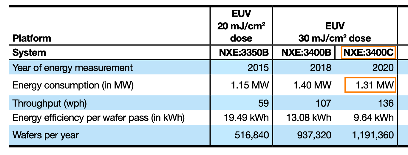
We refer to two sources for the power usage of particular scanner models. The first is on page 68 ASML’s 2020 annual report which suggests that at 100% untilization, the NXE:3400C consumes 1.31MW. While we don’t have exact figures for the NXE:3800D, but Jones 2023 and media reports suggest its about the same accounting for increased complexity of more advanced manufacturing processes and increased efficiency of later models.
Assuming each phase consumes 200MW of power, scanners account for 11% of that usage, and and each scanner consumes 80% x 1.31MW, the eight fab phases at TSMC Fab 18 support 167 scanners. This shows internal consistency across the two modeling approaches for the number of units. The subsequent throughput analysis is rests on the same assumptions of scanner throughput, so we should expect the results to be broadly consistent from this point on.
Using the time series of phase construction, we get the estimate of production capacity in the results section above.
Conclusions
In general, the methodologies in this report assume high utilization, mature throughput, and an averaged product mix. Each of those assumptions biases the estimates up, so these capacity estimates are more like a practical upper bound than an estimate of the actual realizable output.
In some ways analyzing the production capacity of TSMC is simpler than analyzing the capacity of its competitors. TSMC is a pure fab: it’s entire business is manufacturing chips for other companies. While one business line at Samsung and Intel is operating a fab for other semiconductor firms, a substantial portion of their revenues come from semiconductors they design and market themselves. Thus, the revenue reporting of TSMC maps relatively cleanly to production capacity of a commoditized product. Secondly, the scanner tracking analysis is facilitated by the fact that one of the reported geographic revenue categories from ASML is strongly associated with TSMC. Many companies operatie fabs in Europe and North America, and which makes attributing scanner sales to those geographic regions more difficult. In the future as TSMC grows their manufacturing capacity in the United States, this analysis could become more difficult or less reliable.
Many aspects of this analysis could be refined or improved, especially with access to superior data sources. Some of the major sources of uncertainty are:
- ASP dispersion across customers and product type and how AI devices might differ from “average” products
- Factors involved in scanner utilization, downtime, rescans, scanner installation ramp-up and other details of the actual production process. This is handled by a single “utilization” factor which is very approximate.
- Exposure counts per wafer
- The specific scanner models utilized in specific fabs
The analysis for this project was coded by Ryan McCorvie in R. The source code may be found in the [fabanalysis] project on github.